ZnO Wafer, CdS wafer, CdSe wafer, CdTe wafer, ZnS wafer, ZnSe wafer and ZnTe wafer
We provides high purity single crystal ZnO wafer and ZnO bulk for power device , LED , sensor and detector applications . With an ideal crystal structure , ZnO wafer ( Zinc oxide ) has a 2% lattice mismatch to GaN , that is much less than the lattice mismatch of sapphire wafer and SiC wafer . ZnO wafer is one of the most suitable substrate for using as GaN epitaxial growth and wide band gap semiconductor application . ZnO wafer are supplied in square shape , undoped , size 10 x 10 x 0.5 mm , double sides polished surface finish and oriented , our high quality ZnO wafer have been widely used for the growth of
nitride base devices . Please contact us for more product information .
ZnO Wafer Application
| GaN epitaxial growth |
UV detectors |
| Power devices |
Light-emitting devices |
| Photovoltaic |
Sensors |
ZnO Wafer Properties
| Chemical formula |
ZnO |
| Crystal structure |
Hexagonal |
| Lattice constant |
3.3 A |
| Lattice mismatch with GaN in <0001> plane |
9 |
| Thermal conductivity |
0.006 cal / cm /K |
| Refractive index |
2.0681 / 2.0510 |
| Identified polished face |
Zn - face / O - face |
Product Specification
| Growth |
Hydrothermal |
| ZnO bulk / block |
26.5 x 26.5 x 10 mm |
| ZnO wafer |
10 x 10 x 0.5 mm |
| Orientation |
Zn face <0001> / O face <000-1> |
| Resistivity |
500 - 1000 ohm-cm |
| Surface |
two sides polished |
| Roughness |
Ra <= 10 A |
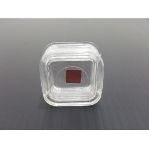
| Package |
Membrance box |