Single Crystal GaP Wafer ( Gallium Phosphide ),widely used as red , yellow , and green LED ( light-emitting diodes )
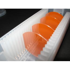
We provides high quality single crystal GaP wafer ( Gallium phosphide ) to electronic and optoelectronic industry in diameter up to 2 inch . Gallium phosphide ( GaP ) crystal is an orange-yellow semi-translucent material formed by two elements , Gallium and Phosphide , growth by Liquid Encapsulated Czochralski ( LEC ) method . GaP wafer is an important semiconductor material which have unique electrical properties as other III-V compound materials and is widely used as red , yellow , and green LED ( light-emitting diodes ) . We have as-cut single crystal GaP wafer for your LPE application , and also provide epi ready grade GaP wafer for your MOCVD & MBE epitaxial application . Please contact us for more product information .
III-V Compound Wafer
We provides a wide range of compound wafer including GaAs wafer, GaP wafer, GaSb wafer, InAs wafer, and InP wafer .
Electrical and Doping Specification
Product Specification
| Growth | LEC |
| Diameter | Ø 2" |
| Thickness | 400 um |
| Orientation | <100> / <111> / <110> or others |
| Off orientation | Off 2° to 10° |
| Surface | One side polished or two sides polished |
| Flat options | EJ or SEMI. Std . |
| TTV | <= 10 um |
| EPD | <= 2E5 cm-2 |
| Grade | Epi polished grade / mechanical grade |
| Package | Single wafer container |