Single crystal and polycrystalline GaAs wafer ( Gallium Arsenide ) for making LD , LED , microwave circuit, solar cell
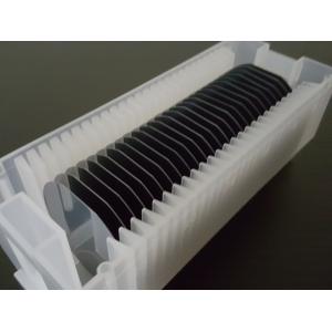
We provides both single crystal and polycrystalline GaAs wafer ( Gallium Arsenide ) to opto-electronics and micro-electronics industry for making LD , LED , microwave circuit and solar cell applications , in diameter range from 2" to 4 ". We offer single crystal GaAs wafer produced by two main growth techniques LEC and VGF method , allowing us to provide customers the widest choice of GaAs material with high uniformity of electrical propertirs and excellent surface quality . Gallium Arsenide can be supplied as ingots and polished wafers , both conducting and semi-insulating GaAs wafer , mechanical grade and epi ready grade are all available . We can offer GaAs wafer with low EPD value and high surface quality suitable for your MOCVD and MBE applications , please contact us for more product information .
GaAs Wafer Feature and Application
| Feature | Application field |
| High electron mobility | Light emitting diodes |
| High frequency | Laser diodes |
| High conversion efficiency | Photovoltaic devices |
| Low power consumption | High Electron Mobility Transistor |
| Direct band gap | Heterojunction Bipolar Transistor |
Product Specification
| Growth | LEC / VGF |
| Diameter | Ø 2" / Ø 3" / Ø 4" |
| Thickness | 350 um ~ 625 um |
| Orientation | <100> / <111> / <110> or others |
| Conductivity | P - type / N - type / Semi-insulating |
| Dopant | Zn / Si / undoped |
| Surface | One side polished or two sides polished |
| Concentration | 1E17 ~ 5E19 cm-3 |
| TTV | <= 10 um |
| Bow / Warp | <= 20 um |
| Grade | Epi polished grade / mechanical grade |